Skip to content
  • Our Work
    • Fields
      • Cardiology
      • ENT
      • Gastro
      • Orthopedics
      • Ophthalmology
      • Pulmonology
      • Surgical Intelligence
      • Surgical Robotics
      • Urology
      • Other
    • Modalities
      • Endoscopy
      • Medical Segmentation
      • Microscopy
      • Ultrasound
  • Success Stories
  • Insights
    • Magazine
    • Upcoming Events
    • Webinars
    • Meetups
    • News
    • Blog
  • The company
    • About us
    • Careers
Menu
  • Our Work
    • Fields
      • Cardiology
      • ENT
      • Gastro
      • Orthopedics
      • Ophthalmology
      • Pulmonology
      • Surgical Intelligence
      • Surgical Robotics
      • Urology
      • Other
    • Modalities
      • Endoscopy
      • Medical Segmentation
      • Microscopy
      • Ultrasound
  • Success Stories
  • Insights
    • Magazine
    • Upcoming Events
    • Webinars
    • Meetups
    • News
    • Blog
  • The company
    • About us
    • Careers
Contact

Visual Inspection of Semiconductors

Imprinting information on a silicon wafer is a complex multi-process task. In the wafer fabrication process, nanoimprinting process miniature patterns a coined on the wafer body using a variety of techniques (such as UV and thermal imprints). Defects can occur during the imprinting process, stemming from air contamination in the vacuum chamber, pressure, uncleaned template, bubble formation due to air trapping and various others.

Visual Inspection of Semiconductors

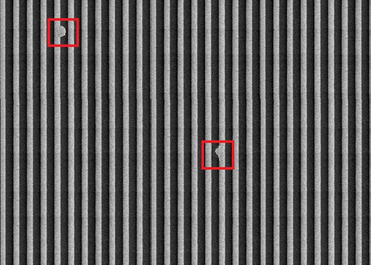
Although improvement in the manufacturing techniques aims at eliminating these defects during production, some defects still remain and can only be visible after wafer manufacturing. A manual scan of a production batch is immensely time consuming and therefore various sensor aided automatic scanning methods have been developed to detect imprint faults and pinpoint defective wafers.

Automatic visual inspection of semiconductors

Automatic detection of wafers and elimination of defective parts in the semiconductor industry is now a part of the routine manufacturing pipeline. The economic implications are obvious: high quality yield is sold in higher price, data reliability increases, faultless parts increase manufacturer’s reputation, and so forth.

Visual inspection of semiconductors is performed using camera mounted on a microscope. The sample wafers are examined by computer vision algorithm and rapidly scanned: the algorithm is designed to quickly detect and classifies defects. In this process, the algorithm can ensure that the right information (template) was reliably imprinted on the silicon wafer.

RSIP Vision has been involved in the construction of reliable chip scanning algorithms to detect and classify faults post manufacture. RSIP Vision developed an advanced software and vision system which conducts image registration and model comparison (among other processes) in its thorough inspection of each reticule, enabling a very fast and accurate visual inspection of semiconductors.

Our detection software saves our client money and effort through the capture of critical errors early on in the semiconductor production process. At RSIP Vision we’ve been working in the visual inspection field for decades. Please contact us to discuss how we can work together to meet your semiconductor optical inspection requirements.

Share

Share on linkedin
Share on twitter
Share on facebook

Related Content

Percutaneous Nephrolithotomy

PCNL – Planning and real-time navigation

Prostate Tumor Segmentation

Implementing AI to Improve PI-RADS Scoring

RAS Navigation

Tissue Sparing in Robotic Assisted Orthopedic Surgeries

Procedural Planning in urology

Procedural Planning in Urology

C Arm X-Ray Machine Scanner

Radiation Reduction in Robotic Assisted Surgeries (RAS) Using AI

Visible spectrum color

Hyperspectral Imaging for Robotic Assisted Surgery

Show all

RSIP Vision

Field-tested software solutions and custom R&D, to power your next medical products with innovative AI and image analysis capabilities.

Read more about us

Get in touch

Please fill the following form and our experts will be happy to reply to you soon

Recent News

PR – Intra-op Virtual Measurements in Laparoscopic and Robotic-Assisted Surgeries

PR – Non-Invasive Planning of Coronary Intervention

PR – Bladder Panorama Generator and Sparse Reconstruction Tool

PR – Registration Module for Orthopedic Surgery

All news
Upcoming Events
Stay informed for our next events
Subscribe to Our Magazines

Subscribe now and receive the Computer Vision News Magazine every month to your mailbox

 
Subscribe for free
Follow us
Linkedin Twitter Facebook Youtube

contact@rsipvision.com

Terms of Use

Privacy Policy

© All rights reserved to RSIP Vision 2021

Created by Shmulik

  • Our Work
    • title-1
      • Ophthalmology
      • Uncategorized
      • Ophthalmology
      • Pulmonology
      • Cardiology
      • Orthopedics
    • Title-2
      • Orthopedics
  • Success Stories
  • Insights
  • The company