Skip to content
  • Our Work
    • Fields
      • Cardiology
      • ENT
      • Gastro
      • Orthopedics
      • Ophthalmology
      • Pulmonology
      • Surgical Intelligence
      • Surgical Robotics
      • Urology
      • Other
    • Modalities
      • Endoscopy
      • Medical Segmentation
      • Microscopy
      • Ultrasound
  • Success Stories
  • Insights
    • Magazine
    • Upcoming Events
    • Webinars
    • Meetups
    • News
    • Blog
  • The company
    • About us
    • Careers
Menu
  • Our Work
    • Fields
      • Cardiology
      • ENT
      • Gastro
      • Orthopedics
      • Ophthalmology
      • Pulmonology
      • Surgical Intelligence
      • Surgical Robotics
      • Urology
      • Other
    • Modalities
      • Endoscopy
      • Medical Segmentation
      • Microscopy
      • Ultrasound
  • Success Stories
  • Insights
    • Magazine
    • Upcoming Events
    • Webinars
    • Meetups
    • News
    • Blog
  • The company
    • About us
    • Careers
Contact

Wafer defect detection by feature matching

Detection of microscopic defect in wafers and printed circuit boards is a standard procedure in the manufacturing process and also a crucial step in quality assurance. The time consuming human inspection of circuit boards has been replaced in nearly all production lines with an automatic in-line camera-based examination. The regular geometrical shape of the printed boards and wafers renders successful the use of a vision-based detection of anomalies.
Defects or deviations from expected pattern in the wafer can be detected by comparing a finalized product image (end product) to a reference image of a correctly constructed wafer. A pixel-based comparison of the two images can then reveal any deviation of the similarity measure between corresponding pixels in two images and alert for possible defect. Using this approach, false positive detections are reduced only when the two images are within near perfect alignment. Alignment of the two images adds another layer of processing required to deal with changes of resolution, image size, distance from the wafer and matching modalities.
Computer chipset track - with visible defects
Computer chipset track – with visible defects
To reduce the need for alignment and matching acquisition modalities, the reference image and the end product wafer image can be compared on the basis of their image features. A feature in this respect refers to a location in the image having sharp bends and twist and which is invariant to scale and rotation. One such example of image features are the Harris corners features.
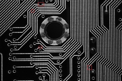
Defects in wafers are many times characterized by an irregular shape on a rather regular geometrical pattern. Such irregularities will attract the feature detector which will mark them as image feature. Along with the defect, normal wafer geometries will be detected as well, such as corners and bends in the microscopic structure of the reference image.

The road to wafer defect detection

The problem of wafer defect detection is then reduced to matching only several candidate features instead of the whole image. By this approach, a pixel by pixel comparison is avoided, making the use of this approach very attractive both for in-line and off-line examination of wafers for defects. In general, the group of features extracted from the reference and end product image should not be equal. Therefore, combinatorial algorithms need first to match pairs of features in the reference image to those found in the end product.
Mismatched, missing or additional features need closer inspection in order to determine if they are indeed defects. At this point, tailor-made algorithms constructed for the geometry under study are needed in order to detect only those mismatched features which are indispensable for a correct wafer defect detection.
Once the performance of the defect detector is considered satisfying, characterization of the defects can take place. Defects of one type or another can indicate malfunctions in specific location along the manufacturing line. Such an occurrence would allow the factory engineers to pinpoint problematic machinery and replace it. Furthermore, defect classification can aid assessing the severity of the damage of a defective part and formulating decisions regarding its fate.
A great expertise is required in order to detect and classify defects the size of which might span less than a fraction of a percentage of the image size. A failure to detect them might lead to severe consequences both in terms of product reliability and usability. At RSIP Vision we have been working with the semiconductor industry for two decades. Our in-house expertise allows us to construct state of the art vision-based algorithms, which were successfully embedded in industrial machinery. Visit our section on semiconductors to learn more.

Share

Share on linkedin
Share on twitter
Share on facebook

Related Content

Percutaneous Nephrolithotomy

PCNL – Planning and real-time navigation

Prostate Tumor Segmentation

Implementing AI to Improve PI-RADS Scoring

RAS Navigation

Tissue Sparing in Robotic Assisted Orthopedic Surgeries

Procedural Planning in urology

Procedural Planning in Urology

C Arm X-Ray Machine Scanner

Radiation Reduction in Robotic Assisted Surgeries (RAS) Using AI

Visible spectrum color

Hyperspectral Imaging for Robotic Assisted Surgery

Show all

RSIP Vision

Field-tested software solutions and custom R&D, to power your next medical products with innovative AI and image analysis capabilities.

Read more about us

Get in touch

Please fill the following form and our experts will be happy to reply to you soon

Recent News

PR – Intra-op Virtual Measurements in Laparoscopic and Robotic-Assisted Surgeries

PR – Non-Invasive Planning of Coronary Intervention

PR – Bladder Panorama Generator and Sparse Reconstruction Tool

PR – Registration Module for Orthopedic Surgery

All news
Upcoming Events
Stay informed for our next events
Subscribe to Our Magazines

Subscribe now and receive the Computer Vision News Magazine every month to your mailbox

 
Subscribe for free
Follow us
Linkedin Twitter Facebook Youtube

contact@rsipvision.com

Terms of Use

Privacy Policy

© All rights reserved to RSIP Vision 2021

Created by Shmulik

  • Our Work
    • title-1
      • Ophthalmology
      • Uncategorized
      • Ophthalmology
      • Pulmonology
      • Cardiology
      • Orthopedics
    • Title-2
      • Orthopedics
  • Success Stories
  • Insights
  • The company